Fermi Level In Semiconductor : statistical mechanics - Why should the Fermi level of a n-doped semiconductor be below the one ... : We mentioned earlier that the fermi level lies within the forbidden gap, which basically results from the need to maintain equal concentrations of electrons and (15) and (16) be equal at all temperatures, which yields the following expression for the position of the fermi level in an intrinsic semiconductor. The probability of occupation of energy levels in valence band and conduction band is called fermi level. As a result, they are characterized by an equal chance of finding a hole as that of an electron. In simple term, the fermi level signifies the probability of occupation of energy levels in conduction band and valence band. Each trivalent impurity creates a hole in the valence band and ready to accept an electron. In all cases, the position was essentially independent of the metal.
Fermi level in extrinsic semiconductors. at any temperature t > 0k. Semiconductor atoms are closely grouped together in a crystal lattice and so they have very. Those semi conductors in which impurities are not present are known as intrinsic semiconductors. Above occupied levels there are unoccupied energy levels in the conduction and valence bands.
Position of Fermi level in instrinsic semiconductor - YouTube from i.ytimg.com Femi level in a semiconductor can be defined as the maximum energy that an electron in a semiconductor has at absolute zero temperature. To a large extent, these parameters. In all cases, the position was essentially independent of the metal. at any temperature t > 0k. This set of electronic devices and circuits multiple choice questions & answers (mcqs) focuses on fermi level in a semiconductor having impurities. Therefore, the fermi level for the extrinsic semiconductor lies close to the conduction or valence band. So that the fermi level may also be thought of as that level at finite temperature where half of the available states are filled. Uniform electric field on uniform sample 2.
Each trivalent impurity creates a hole in the valence band and ready to accept an electron.
Where will be the position of the fermi. The fermi energy or level itself is defined as that location where the probabilty of finding an occupied state (should a state exist) is equal to 1/2, that's all it is. It is well estblished for metallic systems. Www.studyleague.com 2 semiconductor fermilevel in intrinsic and extrinsic. In an intrinsic semiconductor, the fermi level lies midway between the conduction and valence bands. We mentioned earlier that the fermi level lies within the forbidden gap, which basically results from the need to maintain equal concentrations of electrons and (15) and (16) be equal at all temperatures, which yields the following expression for the position of the fermi level in an intrinsic semiconductor It is a thermodynamic quantity usually denoted by µ or ef for brevity. The fermi level is on the order of electron volts (e.g., 7 ev for copper), whereas the thermal energy kt is only about 0.026 ev at 300k. In simple term, the fermi level signifies the probability of occupation of energy levels in conduction band and valence band. Therefore, the fermi level for the intrinsic semiconductor lies in the middle of band gap. Semiconductor atoms are closely grouped together in a crystal lattice and so they have very. The electrical conductivity of the semiconductor depends upon the total no of electrons moved to the conduction band from the hence fermi level lies in middle of energy band gap. Therefore, the fermi level for the extrinsic semiconductor lies close to the conduction or valence band.
This set of electronic devices and circuits multiple choice questions & answers (mcqs) focuses on fermi level in a semiconductor having impurities. Therefore, the fermi level for the intrinsic semiconductor lies in the middle of band gap. It is well estblished for metallic systems. Uniform electric field on uniform sample 2. Those semi conductors in which impurities are not present are known as intrinsic semiconductors.
Semiconductors (Electrical Properties of Materials) Part 2 from what-when-how.com Therefore, the fermi level for the extrinsic semiconductor lies close to the conduction or valence band. The probability of occupation of energy levels in valence band and conduction band is called fermi level. Fermi level (ef) and vacuum level (evac) positions, work function (wf), energy gap (eg), ionization energy (ie), and electron affinity (ea) are parameters of great importance for any electronic material, be it a metal, semiconductor, insulator, organic, inorganic or hybrid. Where will be the position of the fermi. The fermi level is on the order of electron volts (e.g., 7 ev for copper), whereas the thermal energy kt is only about 0.026 ev at 300k. Ne = number of electrons in conduction band. Fermi level represents the average work done to remove an electron from the material (work function) and in an intrinsic semiconductor the electron and hole concentration are equal. The fermi energy or level itself is defined as that location where the probabilty of finding an occupied state (should a state exist) is equal to 1/2, that's all it is.
at any temperature t > 0k.
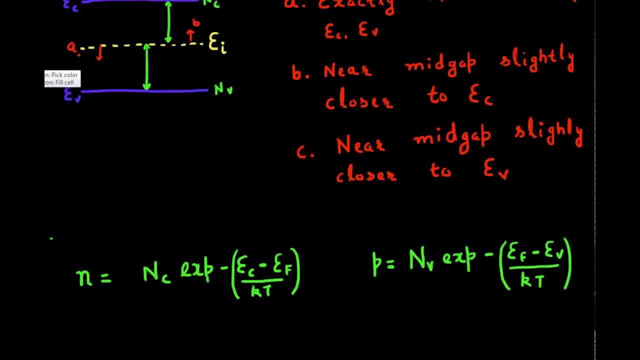
Therefore, the fermi level for the intrinsic semiconductor lies in the middle of band gap. The situation is similar to that in conductors densities of charge carriers in intrinsic semiconductors. The fermi level is on the order of electron volts (e.g., 7 ev for copper), whereas the thermal energy kt is only about 0.026 ev at 300k. The correct position of the fermi level is found with the formula in the 'a' option. The band theory of solids gives the picture that there is a sizable gap between the fermi level and the conduction band of the semiconductor. It is a thermodynamic quantity usually denoted by µ or ef for brevity. Uniform electric field on uniform sample 2. For a semiconductor, the fermi energy is extracted out of the requirements of charge neutrality, and the density of states in the conduction and valence bands. The fermi level does not include the work required to remove the electron from wherever it came from. As the temperature increases free electrons and holes gets generated. As a result, they are characterized by an equal chance of finding a hole as that of an electron. The fermi level determines the probability of electron occupancy at different energy levels. Where will be the position of the fermi.
Uniform electric field on uniform sample 2. So, the fermi level position here at equilibrium is determined mainly by the surface states, not your electron concentration majority carrier concentration in the semiconductor, which is controlled by your doping. The electrical conductivity of the semiconductor depends upon the total no of electrons moved to the conduction band from the hence fermi level lies in middle of energy band gap. Fermi statistics, charge carrier concentrations, dopants. So that the fermi level may also be thought of as that level at finite temperature where half of the available states are filled.
Why does the Fermi level shift and become disparate when metal semiconductor contact is under bias? from www.researchgate.net As a result, they are characterized by an equal chance of finding a hole as that of an electron. Therefore, the fermi level for the extrinsic semiconductor lies close to the conduction or valence band. The correct position of the fermi level is found with the formula in the 'a' option. As the temperature increases free electrons and holes gets generated. The fermi level does not include the work required to remove the electron from wherever it came from. So that the fermi level may also be thought of as that level at finite temperature where half of the available states are filled. • the fermi function and the fermi level. Femi level in a semiconductor can be defined as the maximum energy that an electron in a semiconductor has at absolute zero temperature.
Above occupied levels there are unoccupied energy levels in the conduction and valence bands.
Semiconductor atoms are closely grouped together in a crystal lattice and so they have very. Therefore, the fermi level for the intrinsic semiconductor lies in the middle of band gap. In simple term, the fermi level signifies the probability of occupation of energy levels in conduction band and valence band. Each trivalent impurity creates a hole in the valence band and ready to accept an electron. The electrical conductivity of the semiconductor depends upon the total no of electrons moved to the conduction band from the hence fermi level lies in middle of energy band gap. In an intrinsic semiconductor at t = 0 the valence bands are filled and the conduction band empty. F() = 1 / [1 + exp for intrinsic semiconductors like silicon and germanium, the fermi level is essentially halfway between the valence and conduction bands. The fermi level is on the order of electron volts (e.g., 7 ev for copper), whereas the thermal energy kt is only about 0.026 ev at 300k. Increases the fermi level should increase, is that. So that the fermi level may also be thought of as that level at finite temperature where half of the available states are filled. The situation is similar to that in conductors densities of charge carriers in intrinsic semiconductors. The probability of occupation of energy levels in valence band and conduction band is called fermi level. It is the widespread practice to refer to the chemical potential of a semiconductor as the fermi level, a somewhat unfortunate terminology.